

Differential Amplifier Circuits Based on Carbon Nanotube Field Effect Transistors (CNTFETs)
Sensors, interconnects, and specialty circuits are key applications for CNT-based devices.
Since their discovery, carbon nanotubes (CNTs) have been extensively studied for their great potential in a variety of applications. Several desirable properties that CNTs possess include a high thermal conductivity, high electrical mobility, high electrical current capacity, high tensile strength, small size, compatibility with current semiconductor fabrication processes, and ability to be functionalized.
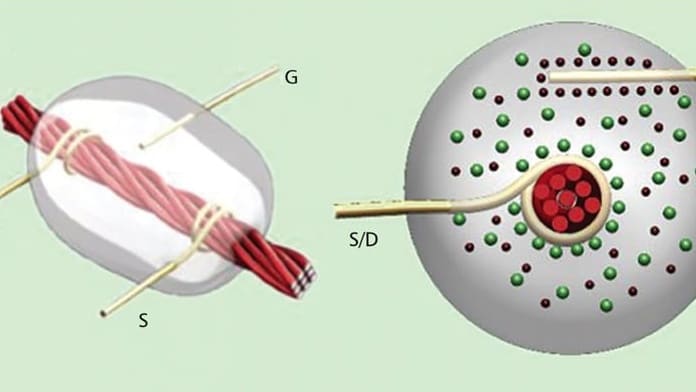
The CNT-based field effect transistor (CNTFET) was demonstrated in 1998, and has opened the door to many avenues of research. Based on the semiconducting, single-walled carbon nanotube (SWNT), CNTFETs display similar behavior to their silicon (Si) metal-oxide-semiconductor FET (MOSFET) equivalents. An oxide film is placed in between a conductive gate and the SWNTs, which acts as the channel of the transistor. Conductive metal contacts on either end of the SWNTs act as the source and drain. A bottom-gate transistor design is typically used, allowing for the SWNT channel to be exposed. This is convenient for sensor applications since the exposed CNT-based channel can be used to detect a variety of analytes via functionalization of the CNTs.
CNT-based sensors take advantage of the chemisorption of compounds onto its surface. The compounds that can be chemisorbed onto the CNT are determined by the functionalization of the CNT. In the case of a CNTFET with an exposed channel, the chemisorption of a particular compound changes the channel conductance of the CNTFET, and thus changes the source-drain current flowing through the device.
The motivation behind this research is to show proof-of-concept circuits for a CNT-based sensor that can eventually be integrated into a portable system carried by a soldier. The circuits would make use of p-channel, depletion-mode transistors built out of SWNTs with metal contacts. Such sensors could potentially be used for detecting chemical and biological agents in the field with a minimal physical and energy footprint, such as an integrated device woven into the uniform or part of an electronics package carried by the soldier.
An important first step in the research was to characterize the current CNTFET devices that the Army Research Laboratory produced in-house. This was done to gain a better understanding of the electrical characteristics and behavior of the devices. It also helped to dictate what applications they could potentially be used in as well as guide fabrication process changes that could potentially improve electrical performance in future CNTFET devices. The devices tested were back-gate, depletion-mode, p-channel FETs with undoped CNT channels and titanium (Ti)-gold (Au) source/drain metal contacts.
Measurements from 151 devices helped provide a good picture of the electrical characteristics for the CNTFETs that were produced thus far, and have provided valuable information for determining improvements that can be made to the device fabrication process. The majority of the CNTFETs currently fabricated typically behave like gate-controlled resistors, with drain-source current leakage occurring most likely due to the presence of metallic carbon nanotubes. Improvements to the fabrication process will be made in hopes of improving the performance of the CNTFETs, and pushing the electrical characteristics closer to that of a silicon-based MOSFET.
The differential amplifier is a base component in many types of active circuits, and it is the foundation for the majority of operational amplifier designs. Differential amplifiers are also used extensively in sensor applications
due to their ability to help amplify small signals and increase the signal-to-noise ratio. It is for these reasons that this research is investigating the construction of CNTFET-based differential amplifier circuits.
Initial differential amplifier measurements were made with a simplistic long-tail design. The initial experiments indicate that a change in the channel conductance is reflected in a change in the output voltage, but this change is not amplified as it typically is for silicon-based differential amplifier circuits. For every 1V difference between the two gates, the output voltage changes on the order of millivolts. Substantially more data will need to be collected and additional experiments will need to be performed to get a better picture of CNTFET-based differential amplifier circuits.
This work was done by Matthew Chin of Oregon State University and Stephen Kilpatrick of the Army Research Laboratory. For more information, download the Technical Support Package (free white paper) at www.defensetechbriefs.com/tsp under the Electronics/Computers category. ARL-0108
This Brief includes a Technical Support Package (TSP).

Differential Amplifier Circuits Based on Carbon Nanotube Field Effect Transistors (CNTFETs)
(reference ARL-0108) is currently available for download from the TSP library.
Don't have an account? Sign up here.
More From SAE Media Group


Tech Briefs
Silicon Carbide High-Voltage Switch
Mobility Engineering
Effects of Differing Carbon Nanotube Field-Effect Transistor Architectures
Electronics & Sensors INSIDER
Leading Experts Suggest Guidelines for Assessing Emerging Transistor Performance

Tech Briefs
Fully Recyclable Printed Electronics


Embedded Technology INSIDER
Could Black Phosphorus be the Next Silicon?


Top Stories
INSIDERDefense
![]() AI Pilots X-62A in First Aerial Dogfight - Mobility Engineering Technology
AI Pilots X-62A in First Aerial Dogfight - Mobility Engineering Technology
INSIDERAerospace
![]() Stratolaunch Approaches Hypersonic Speed in First Powered TA-1 Test Flight -...
Stratolaunch Approaches Hypersonic Speed in First Powered TA-1 Test Flight -...
INSIDERUnmanned Systems
![]() Hermeus Rolls Out First Quarterhorse Hypersonic Test Aircraft - Mobility...
Hermeus Rolls Out First Quarterhorse Hypersonic Test Aircraft - Mobility...
INSIDERManned Systems
![]() Marines Select Prototypes for Light Armored Vehicle Replacement - Mobility...
Marines Select Prototypes for Light Armored Vehicle Replacement - Mobility...
INSIDERMechanical & Fluid Systems
![]() US Navy Taps Hunt Valve for First 3D-Printed Submarine Assemblies - Mobility...
US Navy Taps Hunt Valve for First 3D-Printed Submarine Assemblies - Mobility...
INSIDERAerospace
![]() Two Prototypes Selected for Air Force Collaborative Combat Aircraft Program -...
Two Prototypes Selected for Air Force Collaborative Combat Aircraft Program -...
Webcasts
Power
![]() Transforming Transportation Manufacturing: Unlocking Growth with...
Transforming Transportation Manufacturing: Unlocking Growth with...
Automotive
![]() Accelerating the Software Development Life Cycle for the...
Accelerating the Software Development Life Cycle for the...
Automotive
![]() Applying Model-Based Design to SDV Development: A Practical...
Applying Model-Based Design to SDV Development: A Practical...
Communications
![]() Product Compliance Challenges for Wireless Radio Devices in...
Product Compliance Challenges for Wireless Radio Devices in...
Defense
![]() Building Strong Defenses: Enhancing Supply Chain Resiliency in...
Building Strong Defenses: Enhancing Supply Chain Resiliency in...